
Sample Paper of Digital Electronics
Last Updated: May 19, 2013
sample paper of Digital Electronics
Maximum Marks=100
Time taken=3 hours
Instructions : Attempt any Five questions selecting atleast one from each unit.All questions carry twenty marks each.
Unit 1
1. Explain the working of BCD to Seven Segment decoder.
Ans : This type of decoder accepts the BCD code on its input and provides outputs to energize seven-segment display devices in order to produce a decimal readout.

BCD to Seven Segment Decoder
2. (a) Design gray to binary code converters
Ans : The diagram below shows how gray to binary conversion is done through the use of gates.

3. (a) Compare PMOS with NMOS.
Ans : PMOS is much easier to produce than the n-channel device.PMOS has more than twice the ON resistance of an equivalent NMOS of the same geometry.
(b) Explain CMOS characteristics in detail.
Ans : Power Supply Voltage, Logic Voltage Levels, Noise Margins, Fan out and Power Dissipation are some of the CMOS characterisitcs.
Unit 2
3. (a) Explain BCD Adder in detail with suitable diagrams
Ans : The diagram below explains how a 4-bit binary adder is used to add 2 digits.
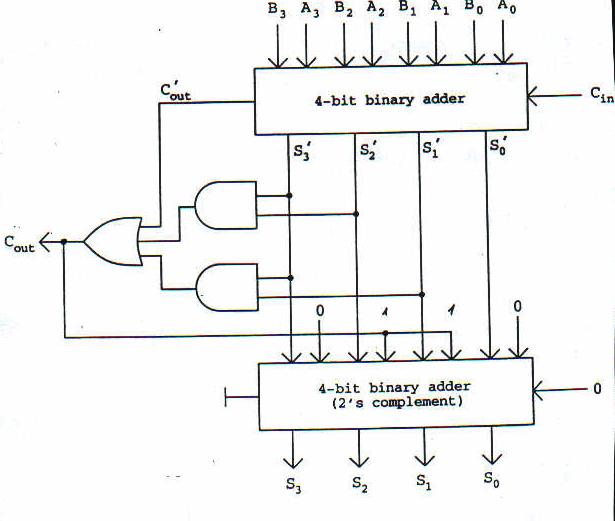
BCD ADDER
(b) Design full adder using mux.
Ans :

Full adder
4. Explain Universal Shift Register in detail.
Ans : This register can work as SISO, SIPO, PISO, PIPO, Left shift register and Right shift register.
Unit 3
5. Define the following terms : (i) Fan out (ii) Operating Temperature (iii) Noise immunity
Ans : Fan out – It is defined as the maximum number of inputs of the same IC family that a gate can drive withou falling outside the specified voltage.Operating Temperature – It is that temperature over which an IC can function properly. Noise Immunity – It is the resistance of the device to unwanted signals or noise while being operational.
6. (a) What is interfacing?
Ans : The output of a circuit/system should match the input of another circuit that has different electrical characteristics.
(b) Discuss the interfacing between CMOS and TTL.
Ans : TTL devices need a supply voltage of 5 V and CMOS devices need it from 3-15V.In order to interface the two several system requirements have to be met.
Unit 4
7. List the various specifications of D/A converters and explain each of them in detail.
Ans : Accuracy, Offset voltage, Settling time, Linearity, Resolution.
8.Explain PLDs in detail with suitable diagrams.
Ans : PLD stands for programmable Logic Devices

PLD
Discover more from Our Education | Best Coaching Institutes Colleges Rank
Subscribe to get the latest posts sent to your email.
« Sample Question For National Institute of Design Sample Paper of Compiler Design »
Tell us Your Queries, Suggestions and Feedback