BPUT Sample Paper for Analog Electronics Circuits
Last Updated: Jul 24, 2013
BPUT SAMPLE PAPER FOR ANALOG ELECTRONICS CIRCUITS
ANALOG ELECTRONICS CIRCUITS
FULL MARKS:-70
Q.1 contains 20 marks (2 marks for each bit) and is compulsory
Q. 2-8 contains 10 marks each ( answer any five)
Q.1
(a) Which h-parameter one can determine from the input characteristics and the output characteristics of a BJT?
Ans:- The parameter hie and hre are determined from the input characteristics while the parameters hfe and hoe are obtained from the output or collector characteristics.
(b) Write down salient features of a voltage series feedback.
Ans:- The salient features of a voltage series feedback are:-
(i) Increase the input impedance
(ii) Increase the Bandwidth
(iii) Decrease the output resistance and non linear distortion.
(iv) Improve characteristic of voltage amplifier.
(c) what are the minimum values of gain in inverting and non-inverting amplifiers?
Ans:- The minimum values of gain in inverting and non-inverting amplifiers are (-RF / R1) and [1 + (RF / R1)] respectively.
(d) Which power amplifier has the maximum efficiency for a given input power? why?
Ans:- Class ‘C’ power amplifier has the maximum efficiency for a given input power, because in this case the output collector current flows for less than half cycle of the input signal i.e. upto 120 degree or 150 degree.
(e) Write down two advantages of push pull amplifier.
Ans:- The advantages of a push-pull amplifier is as follows-
(i) The efficiency of the circuit is quite high.
(ii) Reduced distortion due to the cancellation of even harmonic terms.
(iii) It reduced the humming noise which occurs due to ripple.
(iv) A high ac output power can be obtained.
(f) Why a square wave is fed to an amplifier for testing purpose?
Ans:-The use of square wave testing is significantly less time consuming than applying a series of sinusoidal signals at different frequencies and magnitude to test the frequency response of the amplifier because a square wave is combination of sinusoidal signal with different harmonics. A square wave for the testing process is best described by examining the fourier series expansion.
(g) Which is a better input buffer, a BJT or FET, justify.
Ans:- An FET is a better buffer than BJT because FET has high input impedance in comparison to BJT. We know that if input impedance will be very high then there is no loading effect will be occur.
(h) What is the linear amplification factor of a transistor if its gain is 100?
Ans:- This gain is nothing but “β” value of the transistor.
Hence β=100
Where linear amplification of a transistor is nothing but the current amplification factor “α” of that transistor.
We know that the relationship between α and β i.e.
α = β/(β+1)
or, α = 100/101=0.99
or,α = 0.99
(i) What is diffusion length? what is its importance?
Ans:- Diffusion length for holes is denoted as Lp & Lp = √Dp Ip.
The diffusion length “Lp” represents the distance in to semiconductor at which the injected concentration falls to 1/6 of its value at X=0.
(j) Show that the dynamic resistance of a diode varies inversely with current.
Ans:- We know that Dynamic resistance is nothing but the ac emitter resistance of Emitter base junction diode i.e. re= rac
Where, re=rac = 26 mV / Id = ΔVbe / ΔIe
From the above expression it can be shown that the dynamic resistance of a diode varies inversely with current i.e. rac is directly proportional to 1 / Ie.
2.List the characteristics of an ideal OP-AMP. What is CMRR?
Ans:- The characteristics of an ideal Op-amp are:-
(i) Infinite voltage gain
(ii) Infinite i/p resistance, so that any signal source can drive it .
(iii) Zero o/p resistance, so that o/p can drive an infinite no. of other device.
(iv) Zero o/p voltage when i/p voltages is zero.
(v) Infinite bandwidth
(vi) CMRR= infinite
(vii) Infinite slew rate, so that o/p voltage changes occur simultaneously with i/p voltage changes.
CMRR: Common Mode Rejection Ratio → It is defined as the ratio of differential gain Ad to common mode gain Ac.
Therefore, CMRR = Ad / Ac
Where, Ad= differential mode gain
Ac= Common mode voltage gain
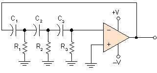
3. Derive the condition for oscillation in a RC phase shift oscillator. Give some advantages and disadvantages of it.
Ans:- For producing oscillations in an oscillator circuit we need positive feedback which means that the voltage signal feedback should be in phase with the input signal.
For providing a +ve feedback network that causes a phase shift of 180 at the desired frequency of oscillation and the 180 phase shift in the feedback signal can be obtained by a suitable network consisting of three RC sections.
f = 1/ 2 π R C √6………..(1)
The corresponding feedback gain is
Β = 1/29……………………(2)
So the circuit will oscillate if
A > 29.
Generally for an oscillator we require 360 degree phase shift. In R.C. phase shift oscillator 180 degree phase shift will occur by using feedback circuit.
It is called as RC phase shift oscillator because 180 degree phase shift has been here by using the combination of resistor and capacitor
→ Rc phase shift oscillator can be done by using BJT or FET or op-amp
As, fo = 1/ 2π√6RC
Thus β= Rf / R1
Merits
- It is cheap and simple circuit as it contains resistors and capacitors.
- It provides good frequency stability.
- The output is sinusoidal that is quite distortion free.
- They have a wide frequency range (few Hz to several hundred kHz)
- They are particularity suitable for low frequencies i.e order of 1 Hz as these frequencies can be easily obtained by using R and C of large values.
Demerits
- The output is small. It is due to smaller feedback.
- It is difficult for the circuit to start oscillation as the feedback is usually small.
RC PHASE SHIFT OSCILLATOR
4. Explain frequency response of BJT amplifiers.
Ans:- Frequency respnose of BJT amplifiers
- The voltage gain of an amplifier varies with signal frequency due to the effect of variations in circuit capacitive reactance with signal frequency on the output voltage.
- The curve drawn between the voltage gain and signal frequency of an amplifier is known as the frequency response. If the input voltage of an amplifier is kept constant but its frequency is varied, it is observed that the amplifier gain.
- The performance of an amplifier depends to a considerable extent upon its frequency response. In the design of an amplifier appropriate steps are taken to ensure that gain is essentially uniform over some specified frequency range.
- In the design of an amplifier appropriate steps are taken ensure that gain is essentially uniform over some specified frequency range.
- A typical graph of amplifier appropriate steps are taken to ensure that gain is essentially uniform over some specified frequency range.
- It is found that the output normally remains constant over a middle range of frequencies and fall off at low and high frequencies
Graph for the frequency response
Here in the graph the low and high frequency are respectively fc1 and fc2. Here the frequency difference is fc1 and fc2 and it is termed as amplifier band width.
The fall off in amplifier gain at low frequency is due to the effect of coupling and bypass capacitor. At medium and high frequencies the capacitive reactance Xc, being equal to 1/ 2πfc is very small and therefore coupling and bypass capacitor behaves as short circuit.
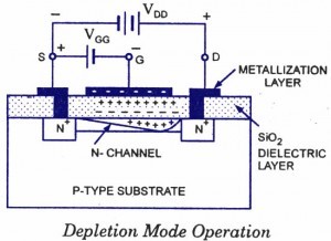
5.Draw and analyze a D-MOSFET configuration. Why is it called so?
Ans:- D-MOSFET is so called because it can e operated in both depletion and enhancement mode by changing polarity of Vgs
→ When –ve gate source voltage is applied the N-channel D-MOSFET operate in the depletion mode.
→ With positive gate voltage it operates in the enhancement mode. Since a channel exist between drain and source ,Id flows even when Vgs = 0. That’s why D-MOSFET is normally known as ON MOSFET.
The basic construction of the n-channel MOSFET is provided above.
- A slab of p-type material is formed from a silicon base and is referred to as the substrate.
- In some cases the substrate is internally connected to the source terminal, however many discrete devices provided an additional terminal resulting in four terminal device.
- The source and drain terminals are connected through metallic contacts to n-doped regions linked by an n-channel.
→ When Vgs = 0, electrons can flow freely from source to drain through the conducting channel which exists between them. When gate is given –ve voltage, it repells the N-channel of its electrons by including +ve charge.
Greater the negative voltage on the gate, greater is the reduction in the reduction in the number of electrons in the channel and consequently lessees its conductivity. Hence, with –ve gate voltage, a D-MOSFET behaves like a JFET and –ve gate operation of a D-MOSFET is called its made operation.
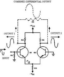
6. What is the need of a differential amplifier? Draw its circuit diagram?
Ans:- Need of differential amplifier:-
- The circuit uses no coupling capacitors. It can works as an amplifier even if the input signal is of very low frequency.
- It can cancel out certain type of undesired voltage signal .i.e. noise.
- If temperature rises both currents Ic1 and Ic2 increase by the same amount. Hence both Vo1 and Vo2 decrease by the same amount. As a result the net output Vo = Vo1 – Vo2 remains the same. Thus the problem of drift does not exist in this circuit.
Circuit diagram of differential amplifier
It has two inputs at Q1 and Q2 from their base. Assume here the voltages are V1 and V2 respectively for Q1 an Q2 and difference between these two voltages .i.e. Vd= V1 –V2 that is effective is controlling the output Vo. Hence the name is differential amplifier.
7.Draw and explain the Op-Amp based integrator.
Ans:-
A circuit in which the output voltage wave form is the integral of the input voltage wave form is the integrator or the integrating amplifier which is shown in figure
Expression for output voltage:
By applying KCL at node V2
I1 = iB + iF
Or, i1 is approx equal to iF because iB is very small
But the current through capacitor is
iC = C × (dvc/ dt)
therefore, (Vin – V2) / R1 = Cf × [d(V2 – V0) / dt]
but V1 = V2 is approximately equal to 0 because a is very large
therefore, Vin / R1 = Cf [d(-Vo) / dt]
The output voltage can be obtained by integrating both sides w.r.t time
Integration of (Vin/R1) w.r.t. dt from 0 to 1 = integration of Cf [d(-V0) / dt] w.r.t dt
=Cf × (-V0) + C
Therefore, V0 = -(1/R1 Cf) × integration of Vin w.r.t. dt + c
Tell us Your Queries, Suggestions and Feedback
5 Responses to BPUT Sample Paper for Analog Electronics Circuits
« Sample Paper for Computer Networks for computer science Sample Paper of Digital Electronics and Circuit »


What is a better input buffer ? Bjt or fet..justify
This is a helpful and an effective set of question paper and helps the students in a broad way. so pls check out this paper and go through it!
The articles contains a important questions.Check this out for the proper guidance.
These are important questions…
one must go through it.
The above article consists of few important questions asked in AEC. This could be helpful for the students in understanding the concepts.