NRAM
Last Updated: Sep 2, 2013
Ques 1. What is NRAM?
Ans. NRAM or Nano-RAM is a proprietary computer memory technology from the company Nantero. It is a type of nonvolatile random access memory based on the mechanical position of carbon nanotube deposited on a chip-like substrate. In theory, the small size of the nanotubes allows for very high density memories. Nantero also refers to it as NRAM.
Ques 2. Explain the technology used in NRAM.
Ans. Nantero’s technology is based on a well-known effect that in a non-woven fabric matrix of carbon nanotubes (CNTs), crossed nanotubes can either be touching or slightly separated depending on their mechanical state. When close to each other, the carbon nanotubes come under the influence of Van der wal’s force. Each NRAM “cell” consists of an interlinked network of CNTs located between two electrodes as illustrated in Fig. The CNT fabric is located between two metal electrodes, which is defined and etched by photolithography and forms the NRAM cell.

Ques 3. What are the characteristics of NRAM?
Ans. NRAM has a density, at least in theory, similar to that of DRAM. DRAM consists of a number of capacitors, which are essentially two small metal plates with a thin insulator between them. NRAM is similar, with the terminals and electrodes being roughly the same size as the plates in a DRAM, the nanotubes between them being so much smaller they add nothing to the overall size. However it seems there is a minimum size at which a DRAM can be built, below which there simply not enough charge is being stored on the plates . NRAM appears to be limited only by the current state of the art in lithography. This means that NRAM may be able to become much denser than DRAM, meaning that it will also be less expensive. Additionally, unlike DRAM, NRAM does not require power to “refresh” it, and will retain its memory even after power is removed. Thus the power needed to write and retain the memory state of the device is much lower than DRAM, which has to build up charge on the cell plates. This means that NRAM will not only compete with DRAM in terms of cost, but will require much less power to run, and as a result also be much faster because write performance is largely determined by the total charge needed. NRAM can theoretically reach performance similar to SRAM, which is faster than DRAM but much less dense, and thus much more expensive.
Ques 4. Explain the working of NRAM.
Ans. To switch the NRAM between states, a small voltage greater than the read voltage is applied between top and bottom electrodes. If the NRAM is in the 0 state, the voltage applied will cause an electrostatic attraction between the CNTs close each other causing a SET operation. After the applied voltage is removed, the CNTs remain in an ON or low resistance state due to physical adhesion (Van der Waals force) with an activation energy (Ea) of approximately 5eV. If the NRAM cell is in the 1 state, applying a voltage greater than the read voltage will generate CNT phonon excitations with sufficient energy to separate the CNT junctions. This is the phonon driven RESET operation. The CNTs remain in the OFF or high resistance state due to the high mechanical stiffness (Youngs modulous 1 TPa) with an activation energy (Ea) much greater than 5 eV. Figure 2 illustrates both states of an individual pair of CNTs involved in the switch operation. Due to the high activation energy (> 5eV) required for switching between states, the NRAM switch shows excellent resistance to outside interference like radiation and operating temperature that can erase or flip conventional memories like DRAM.

Ques 5. Give a brief account on fabricationof NRAM.
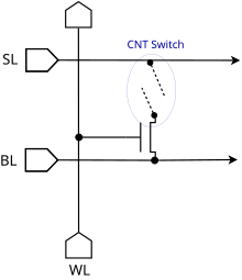
Ans. NRAMs are fabricated by depositing a uniform layer of CNTs onto a prefabricated array of drivers such as transistors as shown in Figure 1. The bottom electrode of the NRAM cell is in contact with the underlying via(electronics) connecting the cell to the driver. The bottom electrode may be fabricated as part of the underlying via or it may be fabricated simultaneously with the NRAM cell, when the cell is photolithographically defined and etched. Before the cell is photolithographically defined and etched, the top electrode is deposited as a metal film onto the CNT layer so that the top metal electrode is patterned and etched during the definition of the NRAM cell. Following the dielectric passivation and fill of the array, the top metal electrode is exposed by etching back the overlying dielectric using a smoothing process such as CMP (chemical-mechanical planarization. With the top electrode exposed, the next level of metal wiring interconnect is fabricated to complete the NRAM array. Figure 3 illustrates one of the many circuit methods that can be used to select a single cell for writing and reading. Using a cross-grid interconnect arrangement, the NRAM and driver, (the cell), forms a memory array similar to other memory arrays such as DRAM or flash memory. A single cell can be selected by applying the proper voltages to the word line (WL), bit line (BL), and select lines (SL) without disturbing the other cells in the array.

Tell us Your Queries, Suggestions and Feedback